Failure Analysis for THT Soldering
Failure Analysis
Design-centric root cause. Simulation - backed answers
THT soldering failures often originate in PCB design decisions. This service provides a Solderability Risk Assessment that links layout and component geometry to thermal behaviour, hole fill, and copper dissolution—using Ishikawa cause–effect mapping supported by soldering simulation.
Especially in automotive, industry, medical and aerospace applications field failure comes at excessive cost and reputation.
Thus, manufacturing quality has to be at highest level possible.
Yet the goal is clearly:
Fast time-to-market,
Higher process robustness,
No rework &
Low manufacturing costs.
Complex THT failures
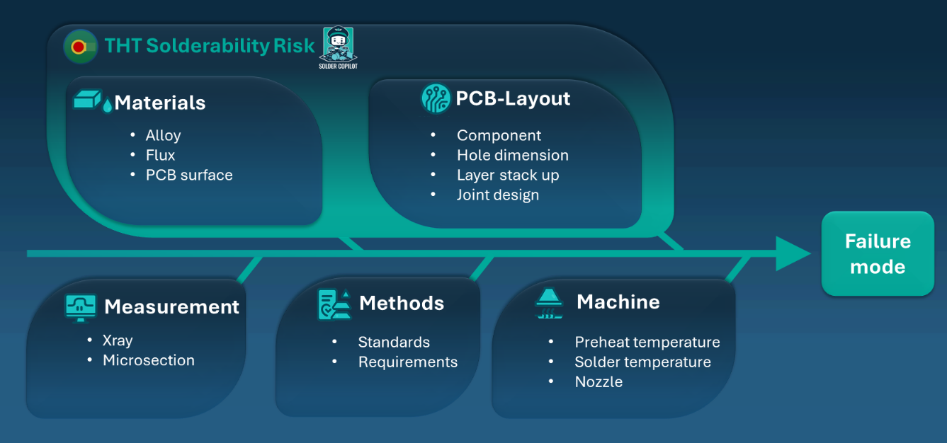
Insufficient hole fill, copper leaching, bridging, voids, non-wetting, and pad lifting interact with:
- PCB design (Gap-Ratio, copper planes, stack-up)
- Materials (surface finish, flux type/solids, alloy)
- Machine parameters (preheat, wave temperature, dwell time, nozzle/N₂)
Design drives failures
Many issues trace back to how heat flows through the joint during selective wave soldering.
- High thermal solder-joint mass (thick barrels, large pins, copper planes) → longer dwell needed → higher copper dissolution risk at the PTH knee.
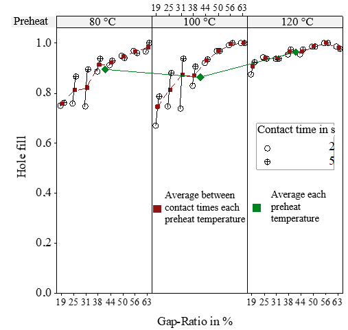
- Tight Gap-Ratio / pin-to-hole clearance + thick stack-ups → reduced vertical flow → lower hole fill unless temperatures rise (again increasing dissolution risk).
- Copper plane attachments / thermal relief patterns → sink heat from the joint → force aggressive profiles.
- Surface finish choice (e.g., NiAu vs. OSP) → changes wetting behavior and thermal margin.
The result: forced machine parameter tweaking instead of fixing the design levers that set the process window.
Simulation driven insights make the difference
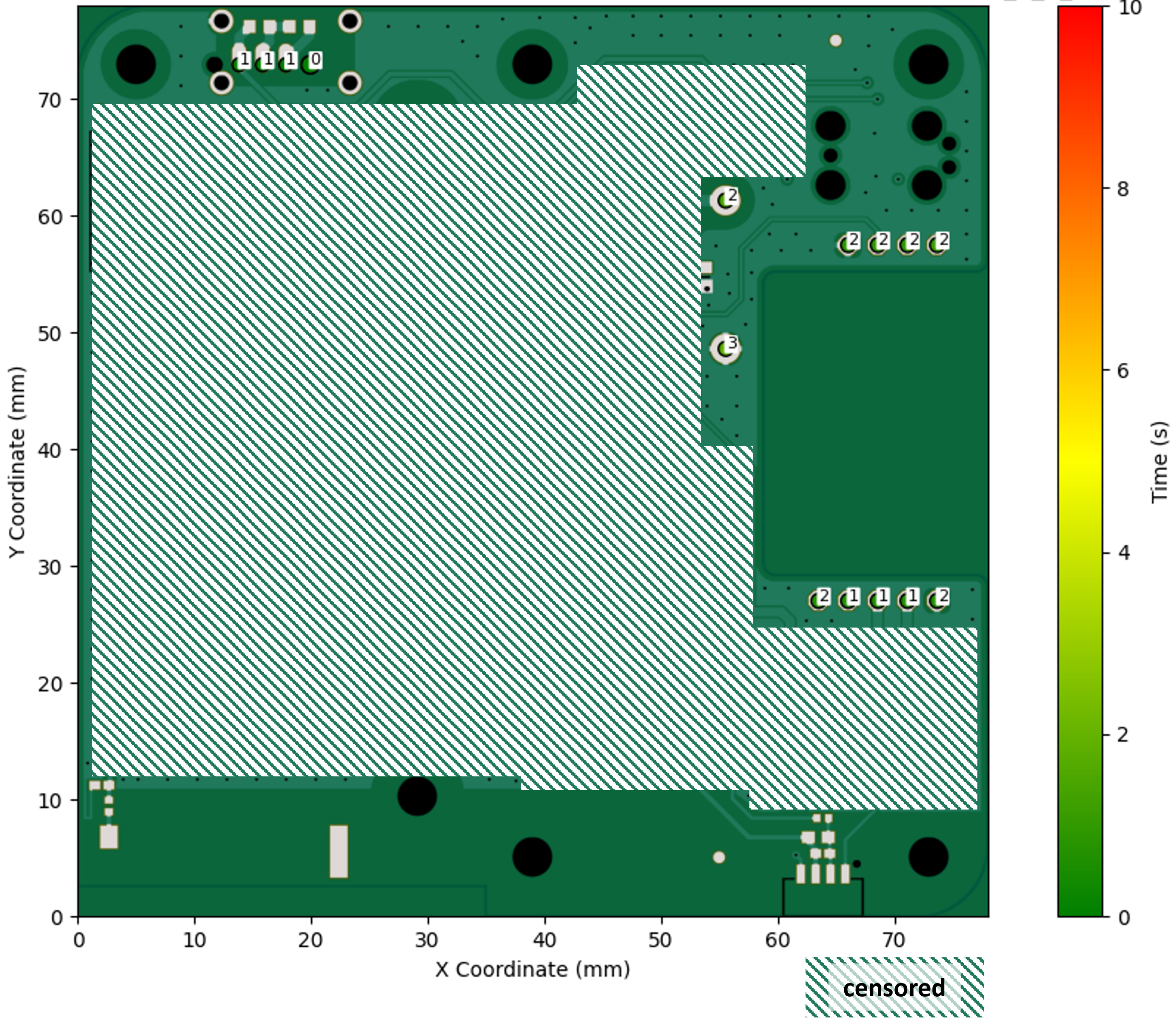
The process behaviour of a THT solder joint layout is core to a meaningful failure analysis.
The solderability risk assessment gives valuable insights into solder joint designs and reveal the risk of insufficient hole-fill or Cu dissolution.
This is a key aspect to draw informed decisions in critical situations without burning time and material.
FAQ
Selective is my specialty but the method also applies to wave and hand soldering for THT-heavy assemblies.
Yes—manufacturability checks from Gerbers/BOM to flag risk joints, advise Gap-Ratio and layout tweaks, and propose starting parameter bands.
All work is under NDA; deliverables can be anonymized for internal distribution.
Typically, an assessment can be delivered within 5–7 working days after receiving your Gerbers, BOM, and process details. Urgent cases can be expedited.
What data do you need to start?
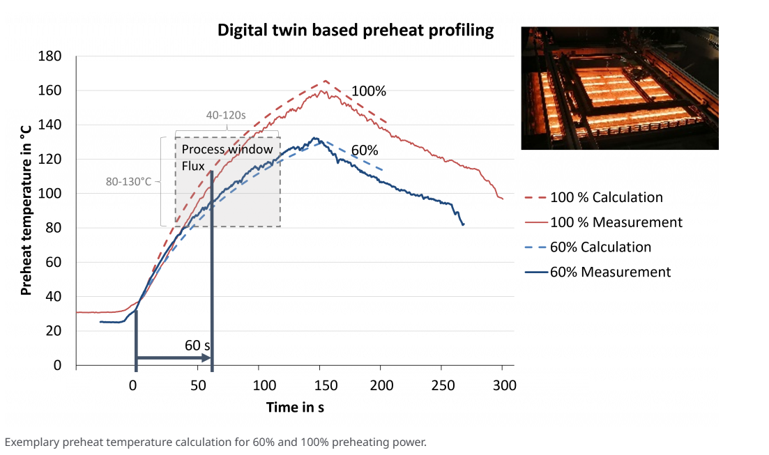
We use your Gerbers, stack-up, finishes, BOM, machine setup, flux, and alloy details to build a digital twin of your process. This ensures accurate risk evaluation by linking design, materials, and process parameters.