THT soldering quality and its standards
Ensuring consistent solder joint quality in through-hole technology (THT) manufacturing is critical for reliable electronic assemblies across different production batches and manufacturing sites. This comprehensive guide explores standardized solder joint quality acceptance criteria, common defect patterns, and quality assessment methods that form the foundation of robust THT soldering processes.
Standardized Acceptance Guidelines
Quality assessment in THT soldering relies on established industry standards and guidelines. These standards, typically specified in manufacturing contracts alongside individual agreements, provide objective criteria for evaluating solder joint quality:
Key Standards
- DIN EN 61192: Requirements for soldered assembly execution quality [57]
- IPC J-STD-001D: Requirements for soldered electrical and electronic assemblies [58]
- IPC-A-610: Acceptance criteria for electronic assemblies [2]
These guidelines are based on optical inspection methods and define tolerances for solder joint anomalies, including form, position, and distance tolerances of solder menisci, component pins, and mounted components.
Assembly Classification System
Electronic assemblies are classified into three categories based on their application requirements:
- Class 1: General Electronics
- Application: Consumer electronics, entertainment devices
- Requirements: Basic functionality only, no reliability requirements
- Class 2: High Reliability
- Application: Industrial control systems, telecommunications
- Requirements: High reliability standards
- Class 3: High Performance Electronics
- Application: Automotive, aerospace, military, safety-critical systems
- Requirements: Maximum reliability and performance standards
Each classification level determines specific acceptance limits for different defect types, with Class 3 having the most stringent requirements.
Automated Inspection in THT Manufacturing
Industrial THT soldering processes rely heavily on automated optical inspection systems [P5] for quality control. AOI systems can detect non-concealed defects and those located within the PCB structure. However, concealed defects require X-ray inspection, and very fine defect patterns may necessitate destructive testing through cross-sections.
The typical defect rate due to statistical manufacturing process variation in soldering is approximately 3,000 ppm [3].
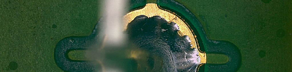
Common THT Solder Joint Defect Patterns
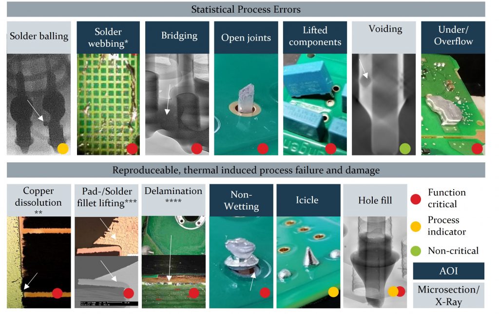
Solder Residue Issues – Solder Balling and Webbing
Solder residue formation, including solder balling and webbing, is influenced by the interaction between solder flow, flux type, and flux quantity [4]. Excessive flux residue alters the adhesion properties of solder mask and affects solder balling and webbing formation [59].
Bridging Defects
Solder bridging occurs when solder solidifies prematurely at incorrect positions, creating unwanted connections between two solder pads. The tendency for bridging depends on flux type and quantity [4, 63]. Bridging occurs preferentially with insufficient flux activity [47].
Factors Promoting Bridging:
- Solder alloy composition: Germanium inhibits bridging [64], while bismuth, copper contamination [65], and dross [66] promote it
- Design factors: Large solder pads and insufficient pin overhang [47, 55]
- Process parameters: Too low preheat temperatures and solder contact times [48]
Solder Icicles
Solder icicles form when heat sources are removed too quickly, causing sudden solder solidification before meniscus formation.
Open Solder Joints
Non-soldered, open solder joints can result from:
- Increased PCB warpage combined with insufficient wave height
- Residual oxides on surfaces due to inadequate flux wetting or activity [35, 67]
- Insufficient heat input for component pins with high thermal mass
- Too low preheat temperature or short solder contact times
Component Lifting
Components can be lifted through:
- Contact with nozzle walls due to PCB warpage or distortion
- Solder flow affecting very light components with large drill holes
Voids in Solder Joints
Voids in THT solder joints are not regulated in the mentioned guidelines. These occur more frequently with lead-free solders than with lead-containing solder alloys. They form particularly in thick PCBs and small solder gaps [68], predominantly at transitions from solder to pin and plated-through holes [69].
Corrosion and Copper Dissolution Issues
The corrosive properties of liquid tin lead to copper dissolution from PCB metallization [71]. Reduced copper cross-section at plated-through holes can result in conductor interruptions and functional failures [72, 73]. The remaining copper thickness is therefore specified in IPC-6012B at 12.3 µm [73] for micro-vias whereas for PTH no minimum thickness is specified. Yet, copper dissolution can lead to serious issues up to product failure.
Thermal Shock Effects
Excessive temperature shocks during contact with the solder wave can cause pad or solder fillet lifting due to different thermal expansion coefficients between copper and epoxy base material (FR4) [61]. Exceeding the heat resistance qualified according to IPC-TM650 can cause delamination between epoxy resin and glass fabric in the base material [62].
PTH Solder hole fill: The Critical Acceptance Criterion
Vertical solder gap filling, known as solder fill height, serves as the primary acceptance criterion for THT solder joints and is significantly influenced by solder joint design [68, P2, P3].
Definition and Calculation
Solder fill height is defined by Formula (1) and evaluated as the quotient of solder height (h) and PCB thickness (l_LP):
Solder Fill Height = h/l_LP** (1)
Acceptance Criteria by Assembly Class
The three standards define consistent acceptance limits for solder fill height (Figure 8). IPC-A-610 is most commonly applied for THT soldering process acceptance.
Target: Complete solder fill height is always desirable. Depending on assembly classification and contractual agreements, lower fill heights may be acceptable.
Critical Applications Requiring 100% Fill
In application-specific cases, solder fill height below 100% is not permitted [2], including:
- Thermal Shock Applications: Assemblies exposed to thermal shock
- High-Frequency (HF) Assemblies: HF behavior changes with insufficient fill height
- High-Current Applications: Current carrying capacity is limited by reduced contact cross-section
In cases with copper layer connection on the PCB top side, current flows only through the metallized copper sleeve of approximately 20-25 µm, which can lead to overheating and fire.
Reliability Implications
Published studies [68, 74-77] confirm the importance of complete solder filling for safety-critical and highly stressed electronics. Thermomechanical alternating loads due to different thermal expansion coefficients (CTE) of solder, copper, and base material [56, 68, 78, 79] cause mechanical stresses in the PCB.
Critical Failure Modes:
- Insufficient solder fill without pin overhang on the solder side leads to early failures [68]
- Vibration loads combined with thermal aging can cause copper layer detachment and fractures in solder, pin, and metallization [74]
Manufacturing Process Considerations
Due to the positioning of THT soldering at the end of the process chain in flat assembly manufacturing, manufacturing-compliant design of THT solder joints is of great importance. Non-conforming soldering frequently leads to destruction of the value creation of all previous manufacturing steps when repair is not permitted or impossible.
Digital Twin Based Process Optimization Strategies
The Solder Copilot, a digital twin of the THT soldering process with simulation-based approaches, can identify problem areas before prototype manufacturing and provide valuable insights into the soldering process. This enables:
- Early defect prediction
- Process parameter optimization
- Design for manufacturability (DfM) validation
- Cost reduction through reduced prototyping iterations
This allows for early detection of potential solderability risks.
For stable processes, modern THT manufacturing integrates:
- Automated optical inspection (AOI) systems
- X-ray inspection for concealed defects
- Machine learning-based quality prediction
- Real-time process monitoring
With these measures stable THT processes at a minimum cost can be realized.
Conclusion
Understanding THT solder joint quality acceptance criteria is essential for manufacturers producing reliable electronic assemblies. By implementing standardized inspection methods, understanding defect patterns, and utilizing modern simulation tools, manufacturers can achieve consistent quality while reducing costs and improving first-pass yields.
The key to success lies in proper design for manufacturability, appropriate process parameter selection, and comprehensive quality control systems that ensure solder fill height requirements are met across all assembly classes.


References
[2] IPC – Association Connecting Electronics Industries. IPC-A-610F, Acceptance criteria for electronic assemblies. Bannockburn/USA
[3] NICOLAE, D. Comparative Study of Through-Hole Soldering Processes [online]. Journal of Electrical and Electronics Engineering, 2021, (14), S. 40-43. Available at: https://search.proquest.com/openview/9528e02da460ceb21073149326f4979a/1?pq-origsite=gscholar&cbl=54417
[4] LIUKKONEN, M., E. HAVIA, H. LEINONEN und Y. HILTUNEN. Application of self-organizing maps in analysis of wave soldering process [online]. Expert Systems with Applications, 2009, 36(3), S. 4604-4609. ISSN 09574174. Available at: doi:10.1016/j.eswa.2008.05.016
[35] DIEPSTRATEN, G. Position Accuracy Machines for Selective Soldering Fine Pitch Components. In: IPC APEX EXPO Proceedings
[47] BATH, J. Lead‐free Soldering Process Development and Reliability: Wiley, 2020. ISBN 9781119482031
[48] MACH, P., P. ZEMAN, E. KOTRCOVA und S. BARTO. Optimization of lead-free wave soldering process using taguchi orthogonal arrays [online]. 3rd Electronics System Integration Technology Conference ESTC, 2010. Available at: doi:10.1109/ESTC.2010.5642946
[55] ARRA, M., D. SHANGGUAN, S. YI, R. THALHAMMER und H. FOCKENBERGER. Development of lead-free wave soldering process [online]. IEEE Transactions on Electronics Packaging Manufacturing, 2002, 25(4), S. 289-299. Available at: doi:10.1109/TEPM.2002.807731
[56] SUNAPPAN, V. und P. COLLIER. Lead-free wave soldering development for pcb assembly. In: 53rd Electronic Components and Technology Conference, 2003. Proceedings: IEEE, 27. Mai 2003, S. 1829-1838. ISBN 0-7803-7791-5
[57] DIN. DIN EN 61192-3: 2003, Requirements for soldered assembly execution quality
[58] IPC – Association Connecting Electronics Industries. IPC J-STD-001: 2005, Requirements for soldered electrical and electronic assemblies. Bannockburn, Ill.: IPC – Association Connecting Electronics Industries
[59] PLATEK, B.T. und S.J. TESARSKI. Susceptibility of solder masks on solderballing and webbing in wave soldering. In: 2008 International Students and Young Scientists Workshop – Photonics and Microsystems: IEEE, 20. Juni 2008 – 22. Juni 2008, S. 59-63. ISBN 978-1-4244-2554-9
[61] HAVIA, E., H. MONTONEN, E. BERNHARDT und M. ALATALO. Comparing SAC and SnCuNi solders in lead-free wave soldering process. In: NEXT Symposium, Finland, 2005
[62] LU, Y., Z. MING, M. LIANG und C. ZHANG. Failure Case Analysis for Abnormal Delamination of Printed Circuit Board. In: International Conference on Quality, Reliability, Risk, Maintenance, and Safety Engineering (QR2MSE), 2019, S. 1-6
[63] DIEPSTRATEN, G. Selective solder fine pitch components on high thermal mass assembly [online]. Available at: https://itweae.com/sites/default/files/technical-papers/SELECTIVE%20SOLDER%20FINE%20PITCH%20COMPONENTS%20ON.pdf
[64] HASNINE, M., B. TOLLA und M. KARASAWA. Effect of Ge addition on wettability, copper dissolution, microstructural and mechanical behavior of SnCu-Ge solder alloy [online]. Journal of Materials Science: Materials in Electronics, 2017, 28(21), S. 16106-16119. ISSN 0957-4522. Available at: doi:10.1007/s10854-017-7511-4
[65] MIYAZAKI, M., S. OGATA, A. YOSHIDA, Y. NISHIYAMA, H. TANAKA, M. AKANUMA und N. KATAYAMA. Influences of Impurities on wave soldering properties for Sn-9Zn solders. In: 4th International Symposium on Environmentally Conscious Design and Inverse Manufacturing, 2005, S. 561-566
[66] TAKEMOTO, T., Y.J. JOO, S. MAWATARI und R. KATO. Reduction of dross formation during wave soldering using lead-free solders. In: Proceedings Second International Symposium on Environmentally Conscious Design and Inverse Manufacturing: IEEE Comput. Soc, 11. Dezember 2001, S. 1131-1136. ISBN 0-7695-1266-6
[67] LIU, X. und L. WANG. Optimization of lead-free wave soldering process for inverter air-conditioner motherboard by DOE. In: 2014 15th International Conference on Electronic Packaging Technology: IEEE, 2014, S. 917-922. ISBN 978-1-4799-4707-2
[68] NGUYEN, J., D. GEIGER, D. ROONEY und D. SHANGGUAN. A study of thermo‐mechanical reliability of lead‐free PTH solder joints [online]. Soldering & Surface Mount Technology, 2009, 21(2), S. 39-47. ISSN 0954-0911. Available at: doi:10.1108/09540910910947462
[69] BIGLARI, M., H., F. KOX, M. HERMANS und KODENTSOV A. Reliability Aspects of Lead-Free Soldering in Industrial Applications. In: Electronic Systemintegration Technology Conference, 2006, S. 481-484
[71] TAKEMOTO, T., T. TAKAHASHI und H. NISHIKAWA. Reduction of copper content from dip-type lead-free soldering bath. In: 2003 EcoDesign 3rd International Symposium on Environmentally Conscious Design and Inverse Manufacturing: IEEE, 12. August 2003 – 12. November 2003, S. 838-842
[72] SNUGOVSKY, P., Z. BAGHERI und C. HAMILTON. Microstructure and Reliability Comparison of Different Pb-Free Alloys Used for Wave Soldering and Rework [online]. Journal of Electronic Materials, 2009, 38(12), S. 2628-2646. ISSN 0361-5235. Available at: doi:10.1007/s11664-009-0923-z
[73] CZAPLICKI, B. Advanced Through-Hole Rework of Thermally Challenging Components/Assemblies: An Evolutionary Process. In: IPC APEX EXPO Proceedings
[74] QI, H., G. PLAZA, S. GANESAN, M. OSTERMAN und M. PECHT. Reliability Assessment on Insertion Mount Assembly under Vibration Conditions. In: 2007 Proceedings 57th Electronic Components and Technology Conference: IEEE, 29. Mai 2007 – 1. Juni 2007, S. 407-414. ISBN 1-4244-0984-5
[75] VIANCO, P.T. und M.K. NEILSEN. Reliability Analysis of Pin-in-Hole Solder Joints by Computational Modeling [online]. Available at: https://www.osti.gov/servlets/purl/1247091
[76] XIAO, H., X. LI, N. LIU und Y. YAN. Failure behavior and life prediction of through-hole solder joints under thermal cycling. In: 2010 11th International Conference on Electronic Packaging Technology & High Density Packaging: IEEE, 16. August 2010 – 19. August 2010, S. 1007-1012. ISBN 978-1-4244-8140-8
[77] BERGER, R., J. OLFE, S. ROGOWSKI, M. RÖLLIG, S. MÜNCH, R. SCHWERZ und H. HEUER. Simulationsgestützte Analyse von Through-hole Technology Verbindungsstellen der Elektronik im Automobilbereich. In: M. NOWOTTNICK, Hg. EBL 2020 – Elektronische Baugruppen und Leiterplatten. Technologische Plattform für die digitale Transformation : Vorträge der 10. DVS/GMM-Tagung, 18.-19. Februar 2020 in Fellbach. Berlin: VDE VERLAG GMBH, 2020. ISBN 978-3-8007-5185-3
[78] SHUJUAN, W., S. XUEJIN, X. SHENGJUN und Z. GUOFU. The numerical simulation and reliability analysis of through-hole solder joints. In: 26th International Conference on Electrical Contacts (ICEC 2012): IET, 14. Mai 2012, S. 443-448. ISBN 978-1-84919-508-9
[79] AKBARI, S., A. LÖVBERG, P.-E. TEGEHALL, K. BRINKFELDT und D. ANDERSSON. Effect of PCB cracks on thermal cycling reliability of passive microelectronic components with single-grained solder joints [online]. Microelectronics Reliability, 2019, 93, S. 61-71. Available at: doi:10.1016/j.microrel.2019.01.006
[P2] SEIDEL, R., T. AHRENS, J. FRIEDRICH, A. REINHARDT und J. FRANKE. Experimental identification and prioritization of design and process parameters on hole fill in mini wave soldering [online]. Microelectronics Reliability, 2022, 131, S. 114497. Available at: doi:10.1016/j.microrel.2022.114497
[P3] SEIDEL, R., M. SIPPEL und J. FRANKE. An Analytical Approach to Thermal Design for Manufacturing in Mini Wave Soldering. In: 2021 IEEE 71st Electronic Components and Technology Conference (ECTC): IEEE, 2021, S. 1427-1434. ISBN 978-1-6654-4097-4
[P5] THIELEN, N., Z. JIANG, K. SCHMIDT, R. SEIDEL, C. VOIGT, A. REINHARDT und J. FRANKE. Clustering of Image Data to Enhance Machine Learning Based Quality Control in THT Manufacturing. In: 2021 IEEE 27th International Symposium for Design and Technology in Electronic Packaging (SIITME): IEEE, 10272021, S. 287-291. ISBN 978-1-6654-2110-2
—
**Keywords:** THT solder joint quality, solder joint acceptance criteria, IPC standards, automated optical inspection, solder fill height, through-hole soldering defects, electronics manufacturing quality control, selective wave soldering, digital twin soldering, solder joint reliability
**Hashtags:** #THTdesign #SolderReliability #ElectronicsManufacturing #SolderingProcess #WaveSoldering #SelectiveSoldering #SMTandTHT #ProcessOptimization #InlineInspection #YieldEngineering #SmartFactory #PCBdesign #HighPowerElectronics #DesignForManufacturing #HardwareStartup #FirstTimeRight #DfMRules #Prototyping #PCBLayoutTips